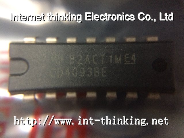
CD4093B consists of four Schmitt-trigger circuits. Each circuit functions as a two-input NAND gate with Schmitt-trigger action on both inputs. The gate switches at different points for positive- and negative-going signals. The difference between the positive voltage (VP) and the negative voltage (VN) is defined as hysteresis voltage (VH) (see Fig. 2).
The CD4093B types are supplied in 14-lead hermetic dual-in-line ceramic packages (F3A suffix), 14-lead dual-in-line plastic packages (E suffix), 14-lead small-outline packages (M, MT, M96, and NSR suffixes), and 14-lead thin shrink small-outline packages (PW and PWR suffixes).
Texas Instruments CD4093BE
cd4093b由四个施密特触发器电路。每个电路起两个输入与非门的作用,在两个输入端都有Schmitt触发器动作。门开关在不同的点,正负信号。正向电压之间的差值(VP)和负电压(越南)被定义为滞后电压(VH)(见图2)。
的cd4093b类型14引线密封双列直插陶瓷封装提供(F3A后缀),14导联线塑料封装(后缀的双E),14引脚小外形封装(M,MT,M96星系,和NSR的后缀),和14引脚超薄紧缩小外形封装(PW和压水堆后缀)。


 | 0 订单数量
 顺丰速运 (https://www.sf-express.com/)
 圆通快递 (https://www.yto.net.cn/)
 中通快递 (https://www.zto.com/)
 顺丰速运 (https://www.sf-express.com/)港澳台
 无需物流 (线下配送)
 规格书
规格书

